Imagine seeing individual atoms lined up in a crystal lattice—details smaller than a single nanometer, far beyond what any optical microscope can reveal. This extraordinary capability is made possible by the transmission electron microscope (TEM), a cornerstone instrument in modern science that enables atomic-scale imaging. Unlike conventional microscopes that use visible light, TEM employs a beam of high-energy electrons to achieve resolutions as fine as 0.2 nanometers, over 1,000 times better than the best optical microscopes.
But how does a transmission electron microscope work? At its core, TEM functions by transmitting electrons through an ultra-thin specimen and capturing how they scatter as they pass through. These interactions are converted into highly detailed 2D images, diffraction patterns, and chemical data, revealing the internal structure, composition, and crystallography of materials at the nanoscale. From analyzing defects in semiconductors to determining the 3D structure of viruses like SARS-CoV-2, TEM has become essential across fields such as materials science, nanotechnology, and structural biology.
In this guide, we’ll break down the full process of how TEM works—from electron generation and beam focusing to image formation, chemical analysis, and advanced techniques. You’ll learn about the critical components, contrast mechanisms, and practical applications that make TEM one of the most powerful tools in scientific research.
Generate High-Energy Electrons at the Source
The first step in TEM imaging is producing a stable, high-energy electron beam. This begins in the electron gun, located at the top of the microscope column. Electrons are emitted from a filament and accelerated downward by a high-voltage potential, typically ranging from 80 to 300 kV. The higher the voltage, the shorter the electron wavelength—thanks to the de Broglie equation:
[
\lambda = \frac{h}{\sqrt{2meV}}
]
where ( h ) is Planck’s constant, ( m ) and ( e ) are the electron mass and charge, and ( V ) is the accelerating voltage. At 200 kV, the electron wavelength is about 0.0025 nm, far shorter than visible light (~400–700 nm), enabling atomic resolution.
Choose Between Thermionic and Field Emission Guns
Two primary types of electron sources are used:
- Thermionic guns heat a tungsten or LaB₆ filament until electrons “boil off” due to thermal energy. These are simpler and more affordable but offer lower brightness and coherence.
- Field emission guns (FEGs) extract electrons from a sharp tungsten tip using a strong electric field, relying on quantum tunneling. They produce brighter, more coherent beams with narrower energy spreads.
FEGs—especially Schottky and cold FEGs—are preferred for high-resolution imaging and spectroscopy due to their superior performance. Cold FEGs provide the highest brightness and smallest energy spread (0.3 eV), while Schottky FEGs offer excellent stability for routine use.
Maintain Ultra-High Vacuum to Protect the Beam
Electrons are easily scattered by air molecules, so the entire TEM column must operate under ultra-high vacuum (UHV)—typically between 10⁻⁵ and 10⁻¹⁰ mbar. Without this, beam coherence would degrade, and imaging quality would collapse.
Use a Multi-Stage Pumping System
To achieve UHV, TEMs employ a layered vacuum strategy:
- Roughing pumps reduce pressure from atmospheric levels to ~0.01 mbar.
- Turbo or diffusion pumps further lower pressure to 10⁻⁷ mbar.
- Ion pumps maintain long-term UHV in the gun chamber without moving parts.
- Differential pumping isolates the electron source using apertures to protect it from contamination.
Samples are introduced via an airlock system, allowing insertion without breaking the main vacuum. Additionally, cryogenic traps cooled by liquid nitrogen capture residual hydrocarbons near the objective lens, preserving image clarity.
Focus the Electron Beam with Magnetic Lenses
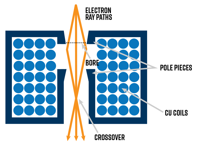
Since electrons can’t be focused by glass lenses, TEM uses electromagnetic lenses—coils surrounded by iron pole pieces—to generate magnetic fields that bend electron trajectories, much like optical lenses bend light.
Control Beam Properties with Condenser Lenses
- Condenser lenses (C1 and C2) shape the beam before it hits the sample.
- In conventional TEM mode, they produce a broad, parallel illumination.
- In STEM mode, they converge the beam into a fine probe.
- A condenser aperture limits beam convergence, improving coherence and reducing aberrations.
Form the Image with the Objective Lens
The objective lens is the most critical component. Positioned just below the sample, it forms the primary image and diffraction pattern:
- The image plane contains the magnified projection of the sample.
- The back focal plane holds the diffraction pattern, crucial for crystallographic analysis.
- Focus is adjusted by moving the sample vertically (via a goniometer), not by changing lens current, to minimize optical distortions.
Magnify the Image with Projector Lenses
After passing through the objective lens, the image is further enlarged by intermediate and projector lenses. These allow variable magnification—from 1,000× up to 50 million ×—depending on the lens settings and mode of operation.
Filter Electrons Using Precision Apertures
Metal discs with tiny holes—called apertures—are inserted into the beam path to select specific electron signals and enhance contrast.
Use Objective Aperture for Contrast Control
- In bright-field (BF) imaging, the aperture allows only unscattered electrons to pass, making thicker or heavier regions appear darker due to mass-thickness contrast.
- In dark-field (DF) imaging, the aperture selects diffracted electrons, highlighting specific crystal orientations or phases.
Isolate Regions with SAD Aperture
The selected area diffraction (SAD) aperture, placed in the image plane, restricts the area contributing to the diffraction pattern. This allows crystallographic analysis of features as small as 0.5 µm in diameter.
Transmit Electrons Through an Ultra-Thin Sample
For electrons to pass through, the sample must be electron-transparent—typically less than 100 nm thick, and even thinner (<10 nm) for high-resolution phase-contrast imaging.
Prepare Samples for Electron Transparency
Different materials require specialized preparation:
- Biological samples: Embedded in resin and cut into 50–70 nm sections using an ultramicrotome.
- Metals: Thinned by electropolishing until electron-transparent.
- Ceramics and semiconductors: Prepared via ion milling with argon ions.
- Site-specific regions: Extracted using focused ion beam (FIB) for targeted analysis.
Caution: FIB can introduce gallium contamination or amorphous layers, potentially distorting results.
Enhance Contrast with Staining and Coating
- Heavy metal stains like uranyl acetate increase electron scattering in biological specimens.
- Carbon or gold coatings prevent charging in non-conductive samples.
Capture Electron-Sample Interactions for Analysis

As electrons pass through the sample, they undergo elastic and inelastic scattering, generating multiple signals used for imaging and spectroscopy.
Detect Elastic Scattering for Diffraction
- Elastic scattering involves no energy loss—electrons are deflected by atomic nuclei.
- In crystalline materials, this follows Bragg’s Law:
[
2d\sin\theta = \lambda
]
where ( d ) is the lattice spacing. The resulting diffraction patterns reveal crystal structure, orientation, and defects.
Analyze Inelastic Scattering for Chemical Data
- Inelastic scattering involves energy loss, producing:
- Characteristic X-rays → detected by EDS (EDX) for elemental identification.
- Energy-loss electrons → analyzed by EELS for bonding, oxidation states, and light elements (e.g., oxygen, carbon).
EELS is especially powerful for analyzing oxides, catalysts, and biological macromolecules due to its sensitivity to fine electronic structure.
Form Images and Diffraction Patterns
TEM provides two fundamental outputs: real-space images and reciprocal-space diffraction patterns, both derived from the same electron beam.
Use Bright-Field and Dark-Field Imaging
- Bright-field (BF): Only unscattered electrons form the image—ideal for general morphology.
- Dark-field (DF): Only diffracted electrons are selected—useful for highlighting specific crystal phases.
Achieve Atomic Resolution with HR-TEM
High-resolution TEM (HR-TEM) uses phase contrast from interference between direct and diffracted beams. This allows visualization of lattice fringes and individual atomic columns—but requires:
- A coherent electron source (FEG)
- Very thin samples (<10 nm)
- Precise focus (Scherzer defocus)
- Stable, vibration-free conditions
Alignment typically takes 10–30 minutes and is sensitive to drift.
Analyze Crystal Structure with SAED
Selected area electron diffraction (SAED) produces patterns showing spots (single crystal), rings (polycrystalline), or halos (amorphous). These are used to identify phases, measure strain, and determine crystal orientation.
Perform Nanoscale Chemical Analysis with EDS and EELS
Beyond imaging, TEM enables elemental and chemical mapping at the nanoscale.
Use EDS for Elemental Identification
- Detects characteristic X-rays emitted when inner-shell electrons are replaced.
- Each element has unique X-ray energies (e.g., Fe Kα = 6.4 keV).
- Limitations: Poor sensitivity for light elements (Z < 11) and limited spatial resolution (~1 µm in thick samples).
Use EELS for Bonding and Oxidation State Analysis
- Measures energy lost by electrons as they pass through the sample.
- Core-loss edges (e.g., oxygen K-edge at 532 eV) identify elements.
- Fine structure (ELNES) reveals oxidation states and bonding environments.
- Advantages: Superior light-element detection and electronic structure information.
Enable Atomic Z-Contrast with STEM Mode

In scanning TEM (STEM), the electron beam is focused into a sub-Ångström probe and scanned across the sample.
Use HAADF-STEM for Z-Contrast Imaging
- The high-angle annular dark-field (HAADF) detector collects electrons scattered at high angles.
- Intensity scales with Z² (atomic number squared), so heavier atoms appear brighter.
- Ideal for identifying dopants, heavy metal labels, or interfaces in complex materials.
Combine with Spectroscopy for Elemental Mapping
- EELS and EDS signals can be collected pixel-by-pixel during scanning.
- Enables atomic-resolution elemental maps, such as mapping Sr, Ti, and O in perovskite oxides.
Achieve Sub-Angstrom Resolution with Aberration Correction
Despite theoretical limits, lens aberrations have historically limited TEM resolution.
Correct Spherical Aberration (Cs)
- Cs causes off-axis electrons to focus too strongly, blurring the image.
- Cs correctors—multipole lenses—compensate for this, enabling sub-Ångström resolution (~0.5 Å).
- Essential for aberration-corrected TEM (AC-TEM), now standard in advanced labs.
Reduce Chromatic Aberration (Cc)
- Cc arises from energy spread in the electron beam.
- Monochromators narrow the energy spread to <0.1 eV, improving EELS resolution and enabling phonon mapping.
Overcome Key Limitations in TEM Imaging
Despite its power, TEM has challenges:
- 2D projections lose depth information—solved using electron tomography (tilt-series reconstruction).
- Beam damage can destroy organic or biological samples—mitigated via cryo-TEM, low-dose imaging, or low-kV operation.
- Vacuum constraints prevent liquid/gas observation—addressed with in-situ holders or Environmental TEM (E-TEM).
Apply TEM Across Scientific Disciplines
TEM’s versatility makes it indispensable:
- Materials science: Study battery degradation, catalyst nanoparticles, and semiconductor defects.
- Nanotechnology: Image graphene, carbon nanotubes, and quantum dots.
- Structural biology: Reconstruct virus structures via cryo-TEM and single-particle analysis—critical in pandemic response.
Final Note: The transmission electron microscope works by generating a high-energy electron beam, focusing it through an ultra-thin sample, and capturing how electrons scatter to form magnified images, diffraction patterns, and chemical data. From the electron gun to aberration correctors and spectroscopic detectors, every component is engineered for atomic-scale precision. While challenges like sample preparation and beam sensitivity remain, continuous advancements in detectors, automation, and in-situ techniques ensure that TEM will remain at the forefront of scientific discovery for years to come.