An electron microscope is a powerful scientific instrument that uses a beam of electrons—instead of light—to produce highly magnified images of specimens at the nanoscale. Because electrons have a much shorter wavelength than visible light, electron microscopes achieve far greater resolution than optical microscopes, allowing scientists to see structures as small as individual atoms. This capability makes electron microscopy essential in fields like biology, materials science, and nanotechnology, where understanding ultrafine details is critical.
Unlike traditional microscopes that use glass lenses and light, electron microscopes rely on electromagnetic or electrostatic lenses to focus electron beams. These instruments operate in a vacuum to prevent electron scattering by air molecules and typically generate grayscale images, which can be colorized digitally for clarity. With the ability to resolve features down to 0.1 nanometers, electron microscopes reveal the invisible architecture of everything from viruses to semiconductor circuits. In this guide, you’ll learn how electron microscopes work, the main types available, their key imaging modes, and where they’re used across science and industry.
Core Function: How Electron Microscopes Work
Electron microscopes generate high-resolution images by using charged particles—electrons—as a source of illumination. The process relies on the wave-like properties of electrons, which have wavelengths thousands of times shorter than visible light, enabling unprecedented magnification and detail.
Electron Beam Generation
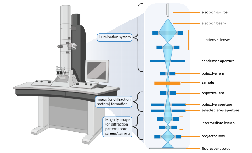
The electron beam starts at the electron gun, located at the top of the microscope column. Common electron sources include:
– Tungsten filament: Inexpensive but lower brightness and shorter lifespan.
– Lanthanum hexaboride (LaB₆): Brighter and more stable than tungsten.
– Field emission gun (FEG): Produces the highest brightness and coherence, essential for atomic-resolution imaging.
Once emitted, electrons are accelerated by a high voltage—typically 20–300 kiloelectron volts (keV)—and focused into a narrow beam using electromagnetic condenser lenses.
Vacuum Environment Requirement
All electron microscopes require a high-vacuum environment inside the column. This prevents electrons from colliding with air molecules, which would scatter the beam and degrade image quality. Most samples must be dry and stable under vacuum, though specialized techniques like environmental SEM allow limited imaging of wet or gaseous samples.
Image Formation Through Electron-Sample Interaction
When the electron beam strikes the specimen, various interactions occur:
– Some electrons pass through (used in TEM).
– Others scatter or emit secondary signals (used in SEM).
– The pattern of transmitted or emitted electrons carries structural, compositional, and crystallographic information.
These signals are captured by detectors and converted into images displayed on a screen. The final image reflects electron density, atomic number, surface topography, or other material properties, depending on the detection method.
Main Types of Electron Microscopes
There are three primary electron microscope designs, each optimized for different applications and sample types.
Transmission Electron Microscope (TEM)
TEM sends a high-energy electron beam through an ultra-thin specimen to create an image based on electron transmission.
What TEM Reveals
- Internal structure of cells, viruses, and materials.
- Crystal lattice arrangements and atomic arrangements in solids.
- Defects like dislocations and grain boundaries.
Key Specifications
- Beam energy: 80–300 keV.
- Resolution: As low as 0.05 nm (50 picometers) in aberration-corrected models.
- Magnification: Up to 50 million times.
- Sample thickness: Must be < 100 nm.
Detection Methods
- Fluorescent screen for real-time viewing.
- CCD or CMOS cameras for digital imaging.
- Direct electron detectors for highest resolution and speed.
TEM is ideal for atomic-scale imaging and structural biology, especially when combined with cryogenic techniques (cryo-TEM).
Scanning Electron Microscope (SEM)
SEM scans a focused electron beam across a sample’s surface and detects emitted signals to produce detailed 3D-like images.
Surface Imaging Advantages
- Excellent topographical contrast—edges and protrusions appear bright.
- Can image larger samples (up to several centimeters).
- Minimal preparation needed for conductive materials.
Detected Signals
- Secondary electrons (SE): Reveal surface shape.
- Backscattered electrons (BSE): Indicate atomic number (Z-contrast).
- X-rays: Enable elemental analysis via EDS.
- Cathodoluminescence (CL): Detect light emission from semiconductors.
Resolution and Limitations
- Typical resolution: 1–20 nm, down to sub-nanometer with field emission guns.
- Non-conductive samples require metal coating (e.g., gold or carbon) to prevent charging.
SEM is widely used in materials inspection, failure analysis, and biological surface studies.
Scanning Transmission Electron Microscope (STEM)
STEM combines scanning and transmission principles, offering analytical power beyond conventional TEM.
How STEM Differs
- A focused beam scans across a thin sample, like in SEM.
- Transmitted electrons are collected, like in TEM.
- Enables Z-contrast imaging using high-angle annular dark-field (HAADF) detectors.
Analytical Strengths
- Simultaneous acquisition of:
- Bright-field and dark-field images
- EDS maps
- EELS spectra
- Perfect for elemental mapping and atomic-resolution spectroscopy.
Drawback
- Data collection is slower due to pixel-by-pixel scanning.
STEM excels in nanomaterials research and semiconductor characterization where precise spatial correlation of structure and chemistry is required.
Imaging Modes and Analytical Techniques
Electron microscopes support multiple imaging and analysis methods tailored to specific scientific questions.
Secondary Electron Imaging (SEM)
Captures low-energy electrons emitted from the top few nanometers of a sample.
- Best for: Surface topography.
- Appearance: 3D-like with strong edge contrast.
- Resolution: < 1 nm with field emission sources.
Use this mode to examine textures, fractures, and surface features in metals, polymers, or biological specimens.
Backscattered Electron Imaging (SEM)
Detects high-energy electrons reflected from deeper within the sample.
- Atomic number sensitivity: Heavier elements appear brighter.
- Topographic contrast possible with directional detectors.
- Segmented BSE detectors allow customizable contrast (e.g., material boundaries).
Ideal for distinguishing phases in alloys or mineral compositions.
Diffraction Contrast Imaging (TEM)
Uses Bragg diffraction of electrons to reveal crystal defects.
Bright-Field vs. Dark-Field
- Bright-field (BF): Transmitted beam forms image; diffracting regions appear dark.
- Dark-field (DF): Diffracted beam selected; only crystalline regions light up.
- Weak-beam dark-field (WBDF): High-resolution imaging of dislocations.
Essential for studying deformation mechanisms and grain structures in materials.
High-Resolution Imaging (HRTEM and STEM)
Reveals atomic arrangements directly.
HRTEM Lattice Imaging
- Interference of multiple diffracted beams creates lattice fringes.
- Interpretation depends on defocus and contrast transfer function (CTF).
- Used to image atomic planes in crystals.
HAADF-STEM Atomic Imaging
- Intensity proportional to atomic number squared (Z²).
- Direct visualization of atomic columns.
- No need for interference conditions—easier to interpret.
Both modes are used in semiconductor defect analysis and 2D material research.
Electron Diffraction
Analyzes crystal structure by examining electron scattering patterns.
Selected Area Electron Diffraction (SAED)
- Parallel beam illuminates a defined area.
- Sharp spots = crystalline material; rings = polycrystalline.
Convergent Beam Electron Diffraction (CBED)
- Focused beam produces diffraction disks.
- Reveals symmetry and space group information.
Precession Electron Diffraction (PED)
- Beam rotates around optic axis.
- Reduces dynamical diffraction effects for easier indexing.
Used in phase identification and crystal orientation mapping.
X-ray Microanalysis (EDS/EDX)
Detects characteristic X-rays emitted when electrons knock out inner-shell electrons.
- Element-specific energies: Each element has unique X-ray peaks.
- Spatial resolution: ~1 μm in SEM; <1 nm in STEM.
- Quantitative analysis possible with standards.
Commonly used to identify contaminants, alloy compositions, or mineral content.
Electron Energy Loss Spectroscopy (EELS)
Measures energy lost by electrons passing through thin samples.
Information Gained
- Elemental composition via core-loss edges.
- Electronic structure from plasmon and bandgap features.
- Chemical bonding via fine structure (ELNES).
Advantages Over EDS
- Better sensitivity for light elements (C, N, O).
- Higher spatial resolution.
- Works best in TEM/STEM with thin samples.
Critical in battery research, catalysis, and quantum material studies.
4D STEM
Records full diffraction patterns at every scan position.
- Data cube: 2D scan + 2D diffraction at each point.
- Enables post-processing for:
- Strain mapping
- Polarization analysis
- Virtual imaging (e.g., dark-field, phase contrast)
Used in studying ferroelectrics, beam-sensitive materials, and complex heterostructures.
Aberration-Corrected Instruments
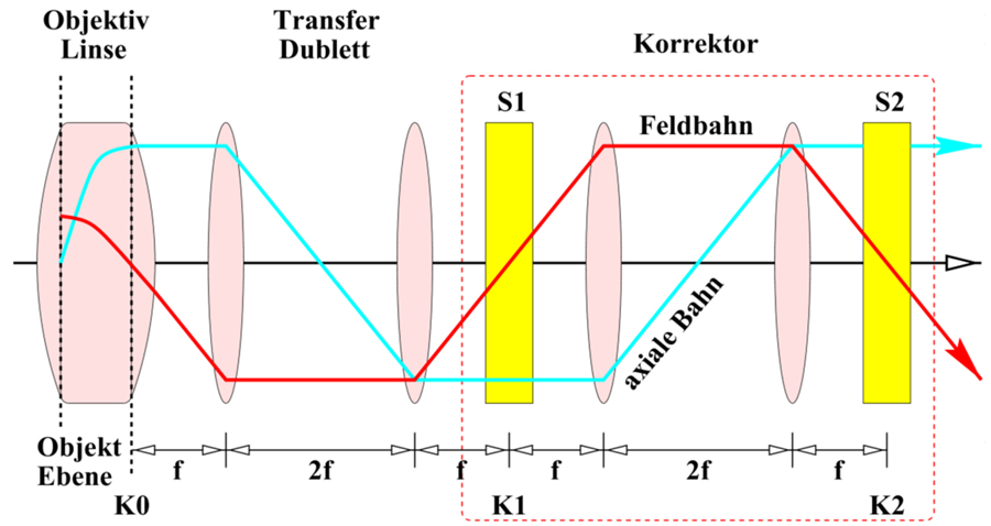
Modern electron microscopes use advanced correctors to overcome inherent optical flaws.
Overcoming Spherical and Chromatic Aberration
Traditional electromagnetic lenses suffer from:
– Spherical aberration: Blurring due to off-axis rays focusing differently.
– Chromatic aberration: Energy spread in electrons causes focus variation.
Corrector Technologies
- Hexapole corrector (Rose & Haider, 1998): For TEM.
- Quadrupole/octupole corrector (Krivanek & Dellby, 1999): For STEM.
These computer-controlled systems reshape the electron beam path to cancel out distortions.
Impact on Resolution
- Resolution improved from ~0.2 nm to < 0.1 nm.
- Now possible to resolve individual atoms in materials like silicon or graphene.
- Standard in high-end TEMs and STEMs as of 2025.
Aberration correction has transformed electron microscopy into a true atomic-scale probe.
Sample Preparation Requirements
Proper preparation is crucial for obtaining accurate, artifact-free images.
General Needs Across Techniques
- Conductivity: Non-conductive samples (e.g., plastics, biological tissue) must be coated with carbon or metal to prevent charging.
- Vacuum stability: Samples must not outgas or degrade under vacuum.
- Cleanliness: Contamination leads to poor imaging and misleading results.
TEM-Specific Methods
Ultramicrotomy
- Embed sample in resin.
- Slice into 70–100 nm sections using diamond or glass knives.
- Common in biological TEM.
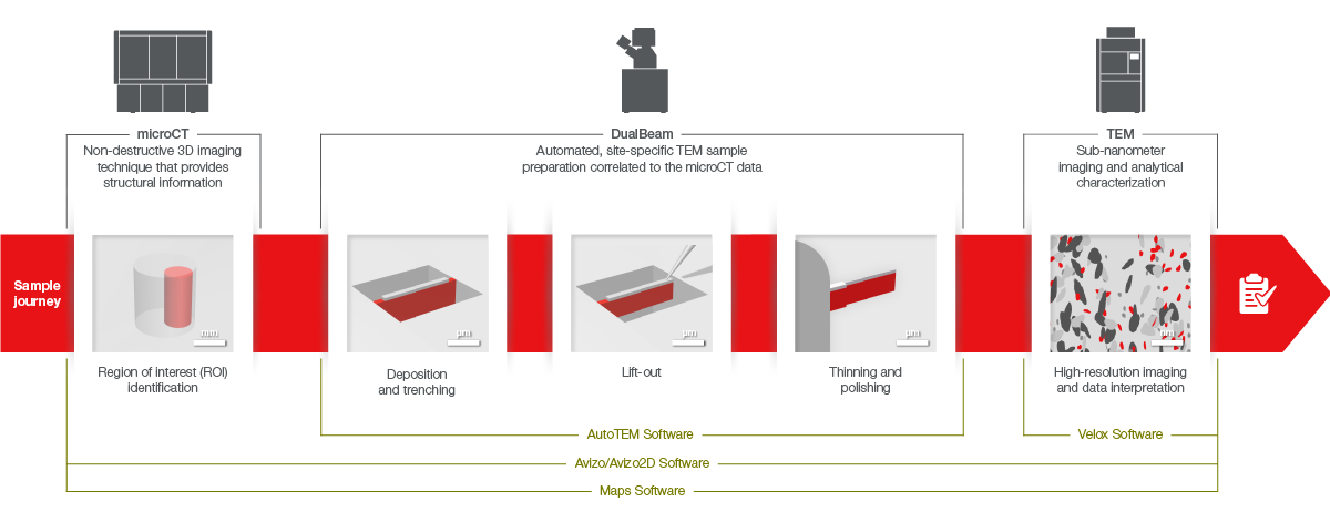
Focused Ion Beam (FIB)
- Use gallium ions to mill thin lamellae from bulk materials.
- Ideal for site-specific analysis in semiconductors or alloys.
Chemical Thinning
- Dissolve material uniformly to reduce thickness.
- Used for metals and some ceramics.
Cryogenic Techniques
Cryofixation and Vitrification
- Rapid freezing (e.g., plunge-freezing in liquid ethane).
- Prevents ice crystal formation, preserving native structure.
- Core of cryo-electron microscopy (cryo-EM).
Used to determine 3D structures of macromolecules without staining or sectioning.
Freeze-Fracture and Freeze-Etching
- Freeze sample, then fracture to expose internal membranes.
- Coat with carbon/metal to create replica.
- Reveals lipid bilayer structure and membrane proteins.
Limitations and Challenges
Despite their power, electron microscopes come with significant constraints.
High Cost and Infrastructure Demands
- Instruments cost $1 million to $10+ million.
- Require:
- Anti-vibration tables
- Magnetic shielding
- Temperature-controlled rooms
- Often housed in dedicated facilities, sometimes underground.
Maintenance and skilled operators add ongoing expenses.
Vacuum and Sample Constraints
Most systems require high vacuum, limiting live biological imaging.
Workarounds
- Environmental SEM (ESEM): Images hydrated samples at low pressure (up to 2.7 kPa).
- Liquid-phase EM: Sealed cells allow observation of nanoparticles growing in solution.
- In situ gas cells: Study catalytic reactions in real time.
These advances enable dynamic studies but are technically complex.
Radiation Damage
High-energy electrons can destroy delicate samples.
Effects Include
- Radiolysis: Breaking of chemical bonds.
- Mass loss: Volatilization of organic material.
- Structural collapse: Especially in proteins and polymers.
Mitigation Strategies
- Low-dose imaging: Minimize exposure time.
- Cryo-cooling: Reduces molecular movement and damage.
- Fast direct detectors: Capture data before degradation.
Critical for biological and soft matter studies.
Artifacts from Preparation
Fixation, dehydration, and staining can distort natural structures.
- Shrinkage, extraction, or precipitation may occur.
- Cryofixation reduces artifacts compared to chemical fixation.
Always interpret results with preparation method in mind.
Applications Across Scientific Fields
Electron microscopes are indispensable tools in modern research and industry.
Biology and Medicine
- Virus imaging: Visualize influenza, HIV, and SARS-CoV-2.
- Cryo-TEM: Determine 3D protein structures at near-atomic resolution.
- Cell ultrastructure: Study mitochondria, nucleus, and cytoskeleton.
Revolutionized structural biology and drug discovery.
Materials Science
- Defect analysis: Dislocations, stacking faults, grain boundaries.
- Phase transformations: Observe changes during heating or stress.
- Nanomaterials: Characterize nanoparticles, nanotubes, and 2D materials like graphene.
Used in developing stronger alloys and advanced composites.
Electronics and Semiconductors
- Circuit inspection: Image features below 5 nm.
- Failure analysis: Locate shorts, voids, or contamination.
- Process control: Monitor etching, deposition, and lithography.
Essential for quality assurance in chip manufacturing.
Geology and Mineralogy
- Mineral identification: Combine imaging with EDS and CL.
- Compositional mapping: Reveal zoning in crystals.
- Meteorite analysis: Study extraterrestrial materials at atomic scale.
Supports planetary science and resource exploration.
Nanotechnology
- Nanodevice fabrication: Image and manipulate quantum dots, nanowires.
- Catalyst design: Study active sites at atomic level.
- In situ TEM: Watch nanoparticles assemble or react in real time.
Drives innovation in energy storage, sensors, and medicine.
Summary: Key Specifications and Capabilities
| Feature | Detail |
|---|---|
| Illumination source | Electron beam (not light) |
| Effective wavelength | ~0.0025 nm at 200 keV |
| Maximum resolution | TEM: < 0.05 nm; SEM: 1–20 nm |
| Max magnification | Up to 50 million× (TEM) |
| Main types | TEM, SEM, STEM |
| Operating environment | High vacuum (mostly) |
| Sample requirements | Thin (TEM), conductive or coated |
| Image output | Grayscale; false color added later |
| Analytical tools | EDS, EELS, electron diffraction, 4D STEM |
Electron microscopes have evolved from early experimental devices to cornerstone instruments in nanoscience. From revealing the double-helix structure of DNA to enabling the development of sub-5nm computer chips, their impact is profound. With ongoing advances in aberration correction, in situ imaging, and computational processing, electron microscopy continues to push the boundaries of what we can see and understand at the smallest scales. Whether you’re exploring the building blocks of life or engineering next-generation materials, the electron microscope remains the ultimate tool for visualizing the invisible.