
Electron microscope resolution is the ultimate measure of clarity in imaging the invisible—determining whether you can distinguish two atoms side by side or resolve the twist of a protein helix. With the ability to visualize structures as small as 40 picometers (0.04 nanometers), modern electron microscopes have shattered the limits of light microscopy and opened the door to atomic-scale science. But despite electrons having wavelengths below 2 pm at high voltages, no microscope achieves resolution at that scale. The gap between theory and reality reveals a deeper truth: resolution isn’t just about physics—it’s an engineering battle against distortion, noise, and instability.
Understanding electron microscope resolution means looking beyond wavelength alone. You’ll learn how aberration correction, detector technology, and sample preparation shape what we actually see. From the quantum behavior of electrons to the seismic hum of city traffic, every factor plays a role. Whether you’re studying catalysts at the atomic level or viral proteins for vaccine design, knowing what limits resolution—and how to overcome it—transforms how you interpret your images and plan your experiments.
How Electron Wavelength Sets the Theoretical Resolution Limit
Electrons as Waves: The de Broglie Principle
The journey to high resolution begins with Louis de Broglie’s revolutionary idea: moving particles behave like waves. For electrons accelerated in a microscope, this means their wavelength shrinks as voltage increases. The de Broglie equation defines this:
$$
\lambda = \frac{h}{mv}
$$
where $ h $ is Planck’s constant, $ m $ is electron mass, and $ v $ is velocity. Higher accelerating voltage increases speed, reducing wavelength. At 200 keV, electrons move at ~70% the speed of light—requiring relativistic corrections that make wavelengths even shorter.
Relativistic Electron Wavelengths at Common Voltages
- 100 keV → 3.70 pm
- 200 keV → 2.51 pm
- 300 keV → 1.96 pm
These values are over 100,000 times smaller than visible light (~550 nm), suggesting picometer-scale resolution should be possible. In contrast, light microscopes hit a wall at ~200 nm due to diffraction.
Yet, no electron microscope reaches λ/2 resolution. Why? Because lens imperfections dominate, not the laws of wave physics.
Why Higher Voltage Improves Resolution
Shorter wavelength directly improves resolving power. Doubling voltage doesn’t double resolution, but it reduces $ \lambda $, allowing finer details to be distinguished. This is why 300 keV TEMs are used for thick biological samples or dense materials—they offer better penetration and theoretical resolution.
However, gains plateau due to increased radiation damage and lens limitations. Most labs use 80–200 keV to balance resolution, contrast, and sample integrity.
Abbe’s Diffraction Limit in Electron Microscopes
Applying Abbe’s Law to TEM Imaging
In an ideal world, resolution follows Abbe’s diffraction limit:
$$
d = \frac{0.612 \lambda}{n \sin \alpha}
$$
With electrons in vacuum ($ n = 1 $) and small aperture angles ($ \alpha \approx 0.01 $ rad), this simplifies to:
$$
d = \frac{0.753}{\alpha V^{1/2}}
$$
where $ d $ is resolution in nm, $ \alpha $ in radians, and $ V $ in volts.
Example: Theoretical Resolution at 100 kV
- Electron wavelength: 3.7 pm
- Using Abbe’s formula: $ d \approx 0.24~\text{nm} $ (2.4 Å)
- With relativistic correction: ~0.22 nm
This is the best-case scenario—achievable only if lenses were perfect and the environment flawlessly stable.
Why Abbe’s Limit Is Not the Real Constraint
Abbe’s law assumes perfect lenses, but electron optics are inherently flawed. Magnetic lenses cannot focus all electrons to a single point. As a result, spherical aberration, not diffraction, sets the real resolution floor in most systems.
Think of it like trying to photograph a fingerprint with a funhouse mirror—the light (or electrons) is good, but the lens distorts everything.
Why Practical Resolution Falls Short of Theory
The Gap Between Wavelength and Performance
| Microscope Type | Theoretical λ | Best Practical Resolution |
|---|---|---|
| Light Microscope | 550 nm | 200 nm |
| Standard TEM | 2.5 pm | 100 pm |
| Aberration-Corrected STEM | 2.5 pm | 40–50 pm |
| SEM | 2.5 pm | 700 pm |
Even with picometer-scale electrons, no system comes close to λ/2. The largest gap is in SEM, where electron scattering in the sample—not optics—blurs the image.
The Core Problem: Imperfect Electron Lenses
Unlike glass lenses, magnetic electron lenses suffer from inherent asymmetry. Electrons passing through the outer edges are bent more than central ones, creating multiple focal points. This spherical aberration smears atomic features into halos.
Without correction, this flaw made atomic imaging impossible—until the 2000s.
Spherical Aberration: The Biggest Barrier to Atomic Imaging
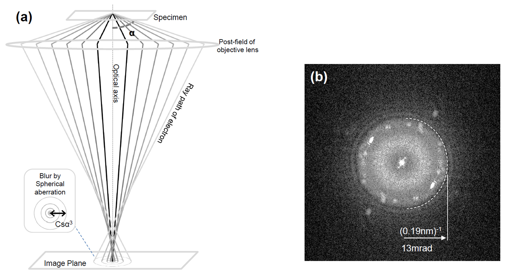
What Causes Spherical Aberration?
In electron lenses, the magnetic field is stronger at the edges, causing off-axis electrons to over-focus. This creates a blurred spot instead of a sharp point. The severity is measured by the Cs coefficient, typically 0.5–2 mm in uncorrected TEMs.
High Cs means worse blurring—equivalent to using a warped lens.
How It Destroys Fine Detail
A 1 Å feature may appear 10x wider due to spherical aberration. This forced early microscopists to use narrow apertures to limit off-axis electrons, sacrificing signal for focus.
It was the primary bottleneck to atomic resolution for decades.
The Coke Bottle Lens Analogy
Imagine trying to read microscopic text through the bottom of a thick, uneven glass bottle. That’s what early TEM was like. Aberration correction is like reshaping that glass in real time—using multipole lenses to cancel out distortion.
This breakthrough enabled sub-50 pm resolution in STEM.
Chromatic Aberration: When Electron Energy Spread Blurs Focus
Why Electron Energy Variability Matters
Not all electrons in the beam have the same energy. This energy spread (1–2 eV) causes chromatic aberration: higher-energy electrons focus differently than lower-energy ones.
Sources include:
– Voltage instability
– Thermal fluctuations
– Inelastic scattering in the sample
Why It’s Worse in Biological Samples
As electrons pass through thick or low-density samples, they lose energy randomly. These varied energy losses defocus the beam, reducing contrast and resolution.
This is especially problematic in cryo-EM, where low-dose imaging limits signal.
How to Correct It
- Omega filters remove inelastically scattered electrons
- Monochromators narrow the energy spread at the source
- Computational methods estimate and remove blur
These tools are critical for near-atomic resolution in soft matter.
Aberration Correction: The Resolution Revolution
Multipole Lenses That Fix Themselves
Modern aberration-corrected microscopes use hexapoles, octopoles, and quadrupoles to dynamically reshape the electron beam. Controlled by software, these elements cancel out spherical and chromatic aberrations in real time.
First developed in the 1990s, they became commercially viable in the 2000s.
Where Aberration Correction Works Best
- STEM: Direct imaging of atomic columns
- HRTEM: Lattice fringes in crystals
- Materials science: Dopants, interfaces, defects
Corrected systems can resolve:
– Single lithium atoms in batteries
– Oxygen columns in oxides
– Bonding in graphene
The Cost of Atomic Clarity
- Instruments cost $5M+
- Require ultra-stable rooms
- Need expert operators
- Sensitive to vibration, EMI, temperature
But for cutting-edge research, they’re essential.
Environmental Stability: Why a Footstep Can Ruin an Image
Vibrations at the Picometer Scale
At atomic resolution, a person walking into the room can shift the sample enough to blur the image. Even distant traffic or HVAC systems introduce noise.
Solutions:
– Floating concrete slabs
– Vibration-damping tables
– Remote operation
Electromagnetic Interference (EMI)
Stray magnetic fields from elevators or power lines deflect electrons. Fields as weak as 1 µT distort images.
Mitigation:
– Mu-metal shielding
– EMI-filtered power
– Careful lab placement
Thermal Drift and Acoustic Noise
A 0.1°C change can move components by nanometers. Acoustic vibrations shake the column.
Fixes:
– Temperature control (±0.1°C)
– Soundproof enclosures
– Hours-long warm-up
Stability isn’t optional—it’s required.
Sample Preparation: The Hidden Limit of Resolution
Fixation Artifacts in Biology
Chemical fixation (glutaraldehyde, osmium) preserves structure but can:
– Shrink membranes
– Aggregate proteins
– Distort organelles
Result: Artifacts mistaken for real biology.
High-Pressure Freezing for Native Structure
Better method: high-pressure freezing at 2000 bar vitrifies water into amorphous ice, preserving native ultrastructure in samples up to 500 µm thick.
Used for C. elegans, tissue slices, and whole cells.
Sectioning and Embedding Matter
Ultrathin sections (30–80 nm) cut with diamond knives must be flawless. Wrinkles, compression, or knife marks degrade resolution.
Choice of resin:
– Epoxy: Best detail
– Acrylic (LR White): Better for immunolabeling
Contrast and Detection: The Final Barriers
Why Biology Lacks Natural Contrast
Light elements (C, H, O, N) scatter electrons weakly. Without staining, biological samples are nearly invisible.
Stains like uranyl acetate and lead citrate boost electron density.
Direct Electron Detectors: The Game Changer
Old detectors used scintillators + CCDs—losing signal. Direct electron detectors (DEDs) capture electrons with higher detective quantum efficiency (DQE).
They enable:
– Movie-mode imaging
– Beam-induced motion correction
– Cryo-EM resolution revolution
DEDs helped cryo-EM reach 3–4 Å, earning the 2017 Nobel Prize.
Final Takeaways: How to Achieve the Best Resolution
Key Limits to Remember
- Spherical aberration – Fixed by correction
- Chromatic effects – Reduced with filters/monochromators
- Environmental noise – Controlled with shielding
- Sample prep – Cryo-freezing > chemical fixation
- Detector quality – Direct > indirect
How to Maximize Your Results
- Use aberration-corrected systems when possible
- Employ DEDs and motion correction
- Optimize sample prep
- Operate in stable environments
- Apply computational processing
The future includes 4D-STEM, in-situ TEM, and AI-driven reconstruction—pushing resolution further than ever. The journey from picometer theory to atomic reality is far from over.